


PPG Signal Acquisition Using the MAX30102 Sensor
1. Theoretical Introduction
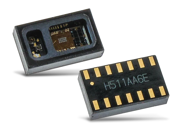
The MAX30102 module (Fig. 1) is an integrated pulse oximetry and heart-rate monitor biosensor module. It includes internal LEDs, photodetectors, optical elements, and low-noise electronics with ambient light rejection. The MAX30102 provides a complete system solution to ease the design-in process for mobile and wearable devices. It operates on a 1.8 V power supply and a separate 3.3 V (typical) power supply for the internal LEDs. The supply voltage for the internal LEDs can be increased up to a maximum of 5 V without risk of damage. The MAX30102 includes an 18-bit ADC and communicates through a standard I2C-compatible interface. The module can be shut down through software with near-zero standby current.
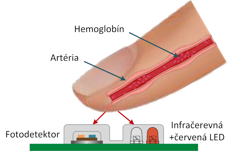
The module acquires the photoplethysmographic (PPG) signal based on the reflective principle (Fig. 2). Subcutaneous tissue illumination is provided by two LEDs with wavelengths of 660 nm (red) and 880 nm (infrared). Utilizing different optical absorption spectra at these wavelengths enables the calculation of blood oxygen saturation; hence, the MAX30102 functions as a pulse oximeter, although it does not calculate this value directly on-chip (it must be computed downstream from the acquired PPG waveforms).
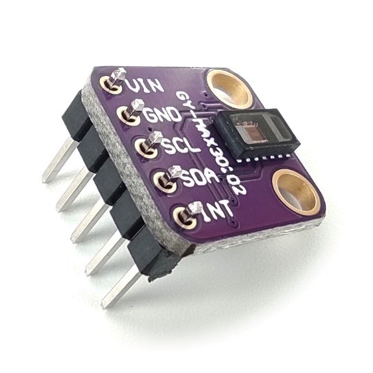
The MAX30102 IC is manufactured exclusively in an SMD package. For rapid prototyping and bench evaluation, it is advantageous to use the IC pre-soldered onto a breakout PCB. In this laboratory exercise, we will use the GY-MAX30102 breakout board (Fig. 3).
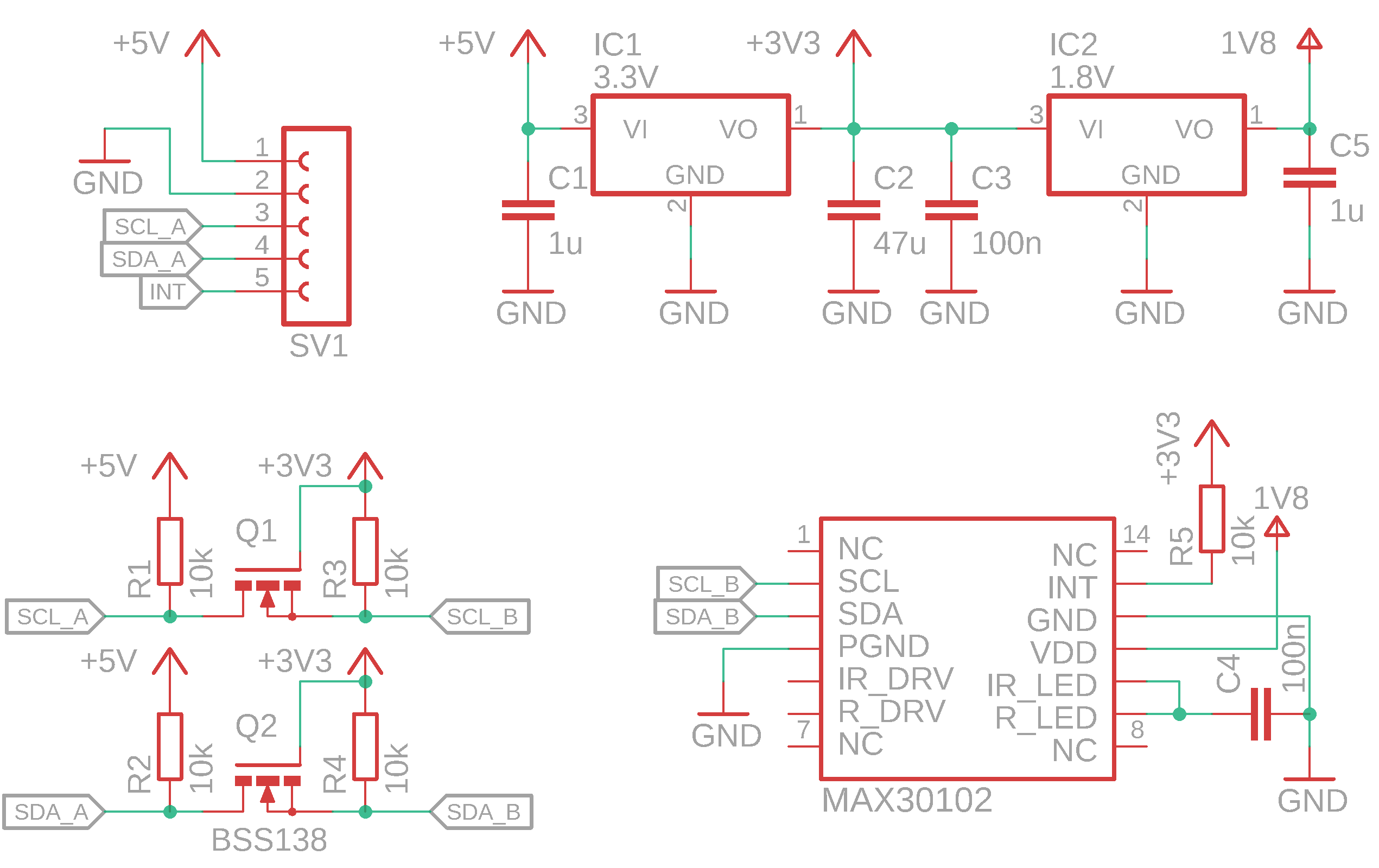
The module can be powered from an input voltage of 5 V or 3.3 V. In addition to the MAX30102 sensor, the breakout board includes onboard low-dropout voltage regulators providing 3.3 V and 1.8 V rails to power the LEDs and the MAX30102 core. It also integrates pull-up resistors, decoupling capacitors, and logic-level shifting circuitry. The schematic diagram is shown in Fig. 4.
1.1 Operating Principle of the Sensor
The analog output from the photodetector is digitized by an on-chip ADC. The maximum resolution of the ADC is 18 bits per sample (nearly three full bytes). Digital samples are queued into a FIFO (First In First Out) circular buffer. Thanks to the buffer, samples do not have to be read out immediately on an individual basis; instead, they can be read in bursts or as an entire buffer dump. The FIFO buffer holds up to 32 sample sets from the Red channel and 32 sample sets from the IR channel. Since each channel sample spans 3 bytes, the maximum capacity of the FIFO buffer is 192 bytes: 32 samples × 3 bytes = 96 bytes for the Red channel and an equal number of bytes for the Infrared channel. The position of the current (most recent) sample in the FIFO is tracked via pointers. Two separate pointers are maintained—a read pointer and a write pointer—allowing sample reads from the buffer to occur asynchronously relative to writes. Detailed FIFO operation and pointer handling are described on page 15 of the datasheet; they will not be elaborated further here, as we will interface with the device using a preconfigured software library.
The sensor operates in two primary operating modes: HR and SpO2. In HR (Heart Rate) mode, only the red LED is pulsed. The mode name stems from the fact that heart rate (HR) can be extracted from a single PPG channel. On common third-party clone modules of the MAX30102, the LED channels are often transposed, meaning the IR LED is pulsed in HR mode instead of the red LED. This applies to the GY-MAX30102 module used in this exercise. In SpO2 mode, both LEDs are actively pulsed. From the dual-wavelength PPG channels acquired from the red and IR LEDs, functional oxygen saturation (SpO2) can be calculated.
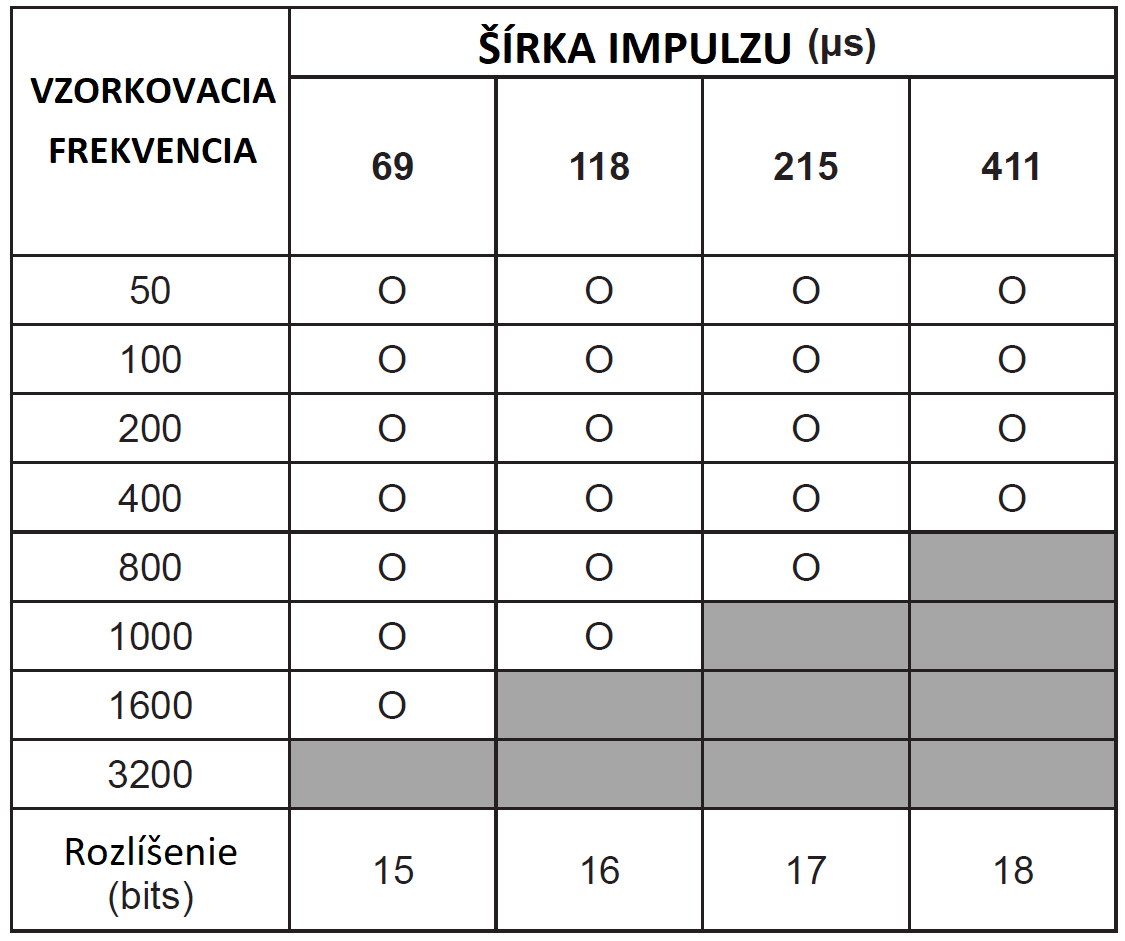
The illuminating LEDs operate in pulsed mode, alternating sequentially in SpO2 mode. During the active LED pulse duration, the photodetector signal is integrated and digitized. A longer pulse width (LED on-time) yields a higher effective bit resolution. The maximum pulse width (411 µs) provides the highest resolution (18-bit). Configurable pulse widths are listed in the table header in Fig. 5. Each decrease in pulse width reduces the ADC resolution by 1 bit. A pulse width of 69 µs yields a 15-bit/sample resolution. The LED pulse width also constrains the maximum achievable sampling rate. The relationship between sampling rate and LED pulse width is illustrated in Fig. 5.
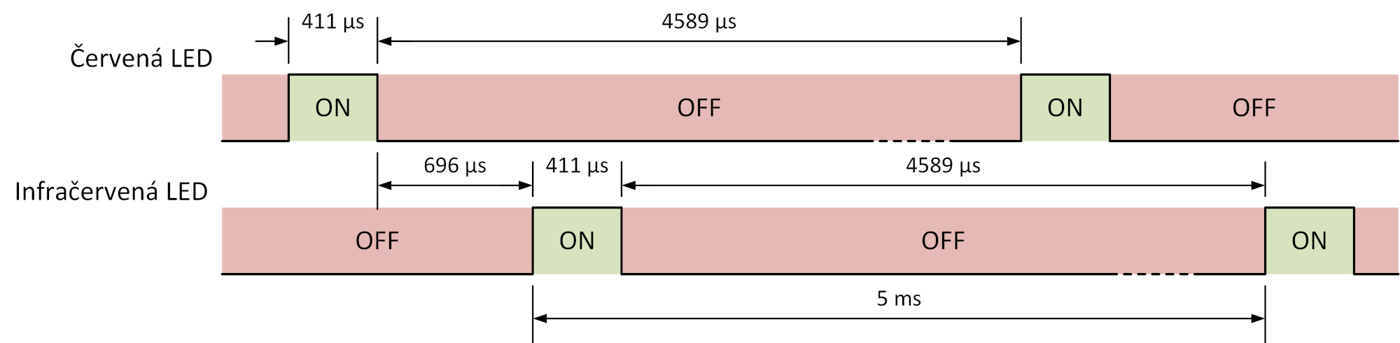
Channel pulsing and timing in SpO2 mode for the maximum pulse width at a 200 Hz sample rate is shown in Fig. 6.
In addition to the operating mode, pulse width, and sampling frequency, users can configure the LED forward drive currents, ADC full-scale range, and digital sample averaging. Onboard sample averaging reduces high-frequency environmental noise. Configuring these parameters is handled via the MAX30102_setup function described in Section 1.3.
1.2 Communication Interface
The MAX30102 communicates over a standard I2C bus, supporting bus clock frequencies up to 400 kHz (Fast mode). The 7-bit slave address for I2C communication is 0x57 (0b1010111).
I2C Write Operation
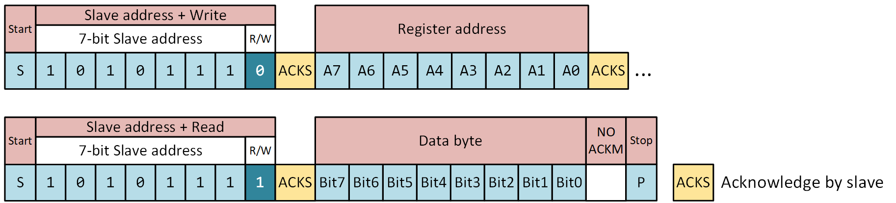
A write transaction begins by transmitting the 7-bit sensor address (Slave address) along with the write bit (R/W = 0), yielding 0b10101110 (0xAE). Next, the target register pointer address (Register address) is transmitted, followed by the configuration payload byte (Data byte). The transaction is terminated with a STOP condition. Writing a single byte is illustrated in Fig. 7.

I2C Read Operation
To read the contents of an internal register, the master must first send the slave address with write mode, i.e., 0b10101110 (0xAE), followed by the register pointer address (Register address) to be accessed. The master then generates a repeated START condition, followed by the slave address with read mode enabled (R/W = 1), i.e., 0b10101111 (0xAF). Following this byte, the sensor shifts out the contents of the addressed register. Finally, the master issues a NACK and a STOP condition. A single-byte read operation is depicted in Fig. 8.
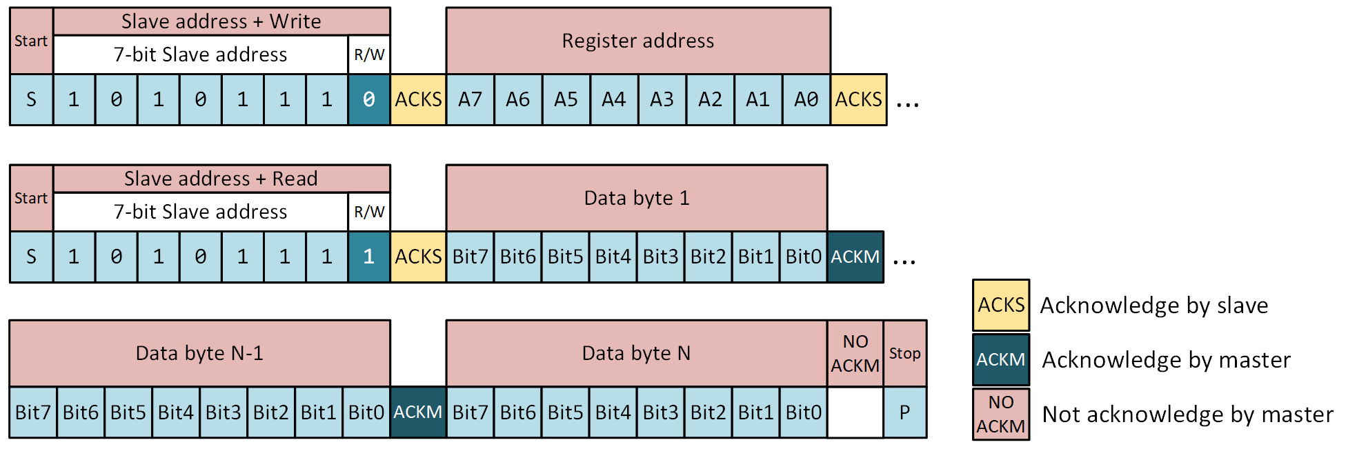
During reads, the internal register pointer auto-increments, allowing consecutive registers or FIFO burst reads without retransmitting the slave or register address. Burst reading continues until the master asserts a NACK and issues a STOP condition. Fig. 9 shows a multi-byte burst read of N bytes starting from the pre-selected register address (Register address).
1.3 Function Library
Numerous operating modes and configuration registers are available on the MAX30102 over the I2C bus. Developing a custom driver from scratch would be time-consuming given the extensive register set. To streamline firmware development, we use the MAX30102.c driver library—an adapted version of the Adafruit driver for AVR microcontrollers. The register definitions and function prototypes are declared in the header file MAX30102.h. The functions utilized in this laboratory exercise are described below:
| Function Declaration | bool MAX30102_init(uint8_t i2caddr) |
| Description | Initializes the I2C peripheral at 400 kHz and reads back the Part ID of the sensor at address i2caddr. |
| Input Parameters | i2caddr – 7-bit I2C address of the MAX30102 left-shifted by 1 bit (0xAE). |
| Return Value | True – sensor ID was verified successfully. False – communication failed or unexpected device ID returned. |
| Function Declaration | void MAX30102_setup(uint8_t powerLevel, uint8_t sampleAverage, uint8_t ledMode, int sampleRate, int pulseWidth, int adcRange) |
| Description | Configures operational registers of the MAX30102. |
| Input Parameters | powerLevel – LED current level configuration. Values: <0 ÷ 255> (0 = 0 mA; 255 = ~50 mA). sampleAverage – Number of adjacent samples averaged in hardware. Values: 1, 2, 4, 8, 16, 32. ledMode – Selects between HR mode (Red LED only) and SpO2 mode (Red + IR LEDs). Values: 1 = HR mode (Red LED) 2 = SpO2 mode (Red + IR LEDs) 3 = Multi-LED mode sampleRate – Sampling rate selection for both channels. Values: 50, 100, 200, 400, 800, 1000, 1600, 3200. pulseWidth – LED pulse width (on-time duration for both LEDs) in [µs]. Values: 69, 118, 215, 411. adcRange – ADC full-scale input current range in [nA]. Values: 2048, 4096, 8192, 16384. |
| Return Value | None |
| Function Declaration | void MAX30102_wakeUp(void) |
| Description | Wakes the MAX30102 from software power-save shutdown mode. |
| Input Parameters | None |
| Return Value | None |
| Function Declaration | void MAX30102_shutDown(void) |
| Description | Places the MAX30102 into ultra-low-power standby shutdown mode. |
| Input Parameters | None |
| Return Value | None |
| Function Declaration | uint16_t MAX30102_check(void) |
| Description | Polls the sensor for new PPG data samples. If new data is ready, it updates the software FIFO circular buffer. This function must be called periodically. |
| Input Parameters | None |
| Return Value | Number of new samples read and queued into the buffer. |
| Function Declaration | uint8_t MAX30102_available(void) |
| Description | Returns the number of unread samples currently available in the software FIFO buffer. |
| Input Parameters | None |
| Return Value | Number of available samples. |
| Function Declaration | uint32_t MAX30102_getFIFORed(void) uint32_t MAX30102_getFIFOIR(void) |
| Description | Retrieves the oldest sample from the FIFO buffer for the Red LED (getFIFORed) and the IR LED (getFIFOIR). |
| Input Parameters | None |
| Return Value | The oldest sample value stored in the FIFO buffer for the corresponding channel. |
| Function Declaration | void MAX30102_nextSample(void) |
| Description | Advances the FIFO head pointer to the next sample. Must be called after reading sample values from the FIFO. In dual-wavelength mode, call this after reading both MAX30102_getFIFORed and MAX30102_getFIFOIR. |
| Input Parameters | None |
| Return Value | None |
| Function Declaration | void MAX30102_timerProc(void) |
| Description | Manages non-blocking timeout delays for I2C and sensor transaction handshakes. This routine must be called inside a periodic timer interrupt every 1 ms. |
| Input Parameters | None |
| Return Value | None |
2. Equipment Used
- Hardware
- Mega Development Board 2 (MDB2)
- MAX30102 PPG sensor breakout board (GY-MAX30102)
- PC
- Software
- MATLAB
- Microchip Studio
3. Schematic Diagram
4. Assignment Tasks
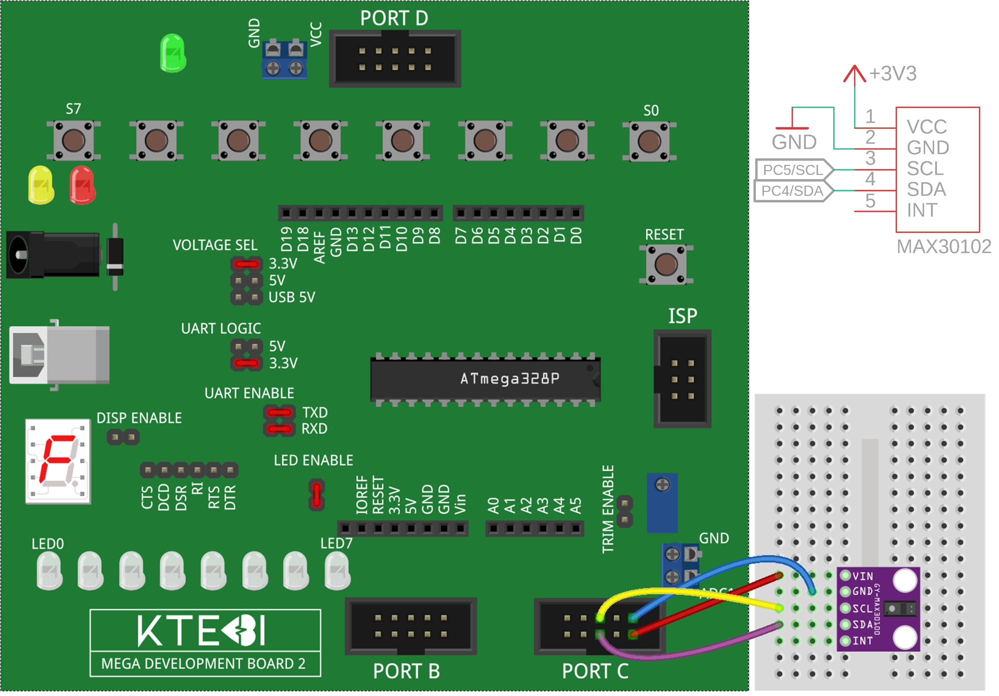
- Connect the MAX30102 sensor module to the MDB2 development board according to the wiring diagram (Fig. 10). Use an external DC power adapter. Jumper positions on the MDB2 board are highlighted in red. Set the sensor supply rail to 3.3 V.
- Write an MCU firmware program in C to acquire PPG signal samples from both LEDs of the MAX30102 sensor and transmit the digitized stream to the PC via UART. Implement the following parameters and features in the code:
- Configure the device for SpO2 mode,
- Set the LED forward current register to 200 (~39 mA),
- Set sample averaging to 2 adjacent PPG samples,
- Set the sampling rate to 200 Hz,
- Set the LED pulse width to 411 µs,
- Set the ADC full-scale current range to 8192 nA,
- Configure the UART baud rate to 76,800 Baud,
- Begin streaming samples to the PC only after receiving the character 'S', and stop transmission upon receiving the character 'X'. Use the UART receive interrupt to detect incoming control commands,
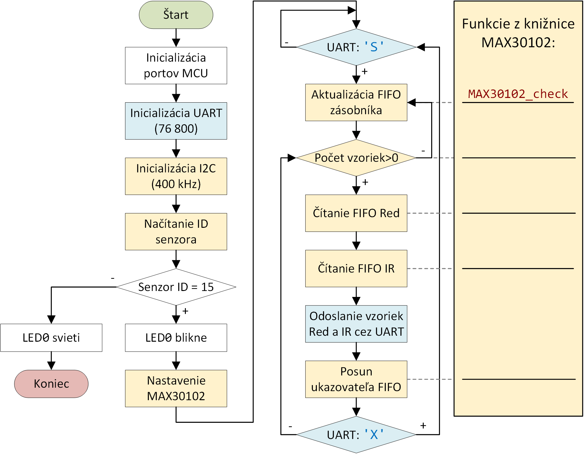
- Structure the program according to the flowchart below:
- In the right-hand column of Fig. 11, write in the corresponding MAX30102 library functions that execute each flowchart block.
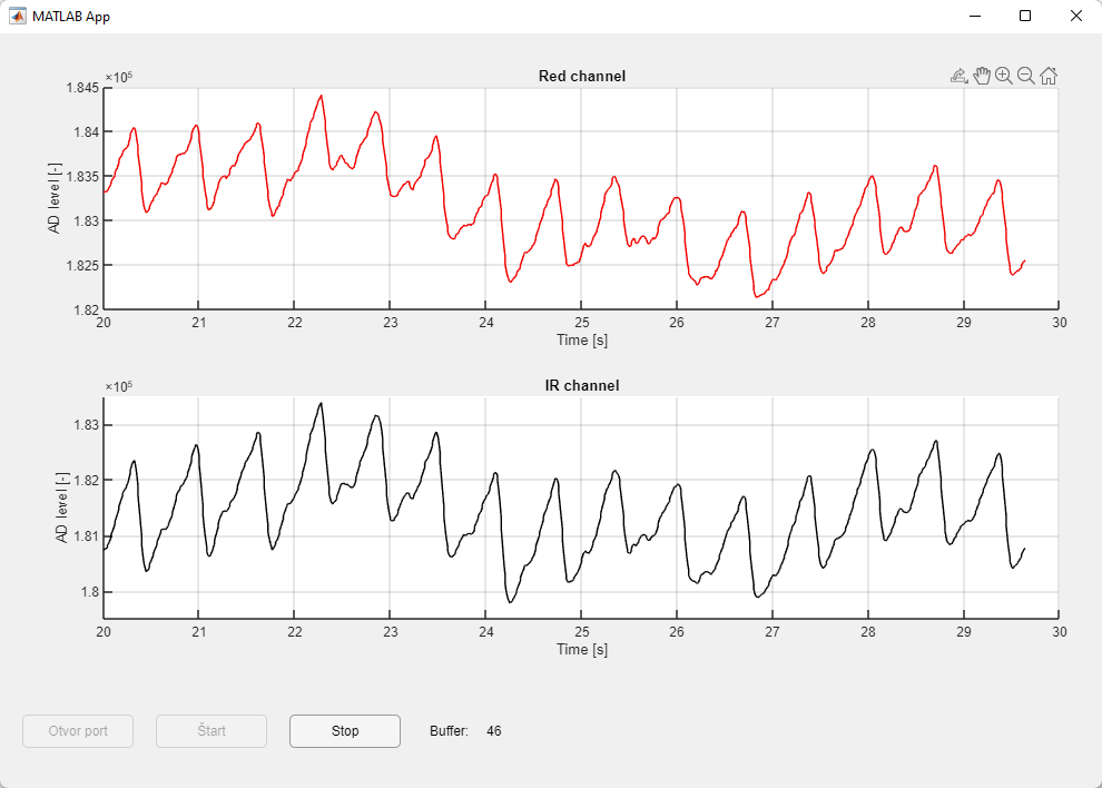
- Develop a graphical user interface application in MATLAB App Designer to display real-time dual-channel PPG waveforms from the Red and Infrared LEDs (Fig. 12). The application must include the following UI elements:
- A numeric/text display showing the serial receive buffer status (byte count),
- Control pushbuttons: 'Open Port', 'Start', and 'Stop'.
- Evaluate the laboratory assignment. Focus on the following points:
- Writing the MCU firmware and resolving implementation bottlenecks,
- Developing the companion MATLAB GUI application.
Downloads
MAX30102.hMAX30102.c