Temperature Measurement Using an SPI Interface Sensor
1. Theoretical Introduction
The sensor operation, electrical schematic diagram, pinout description, and individual register details were presented in the section Temperature Measurement with BMP280 (I2C). Therefore, this theoretical introduction focuses primarily on sensor communication via the SPI interface.
SPI Interface
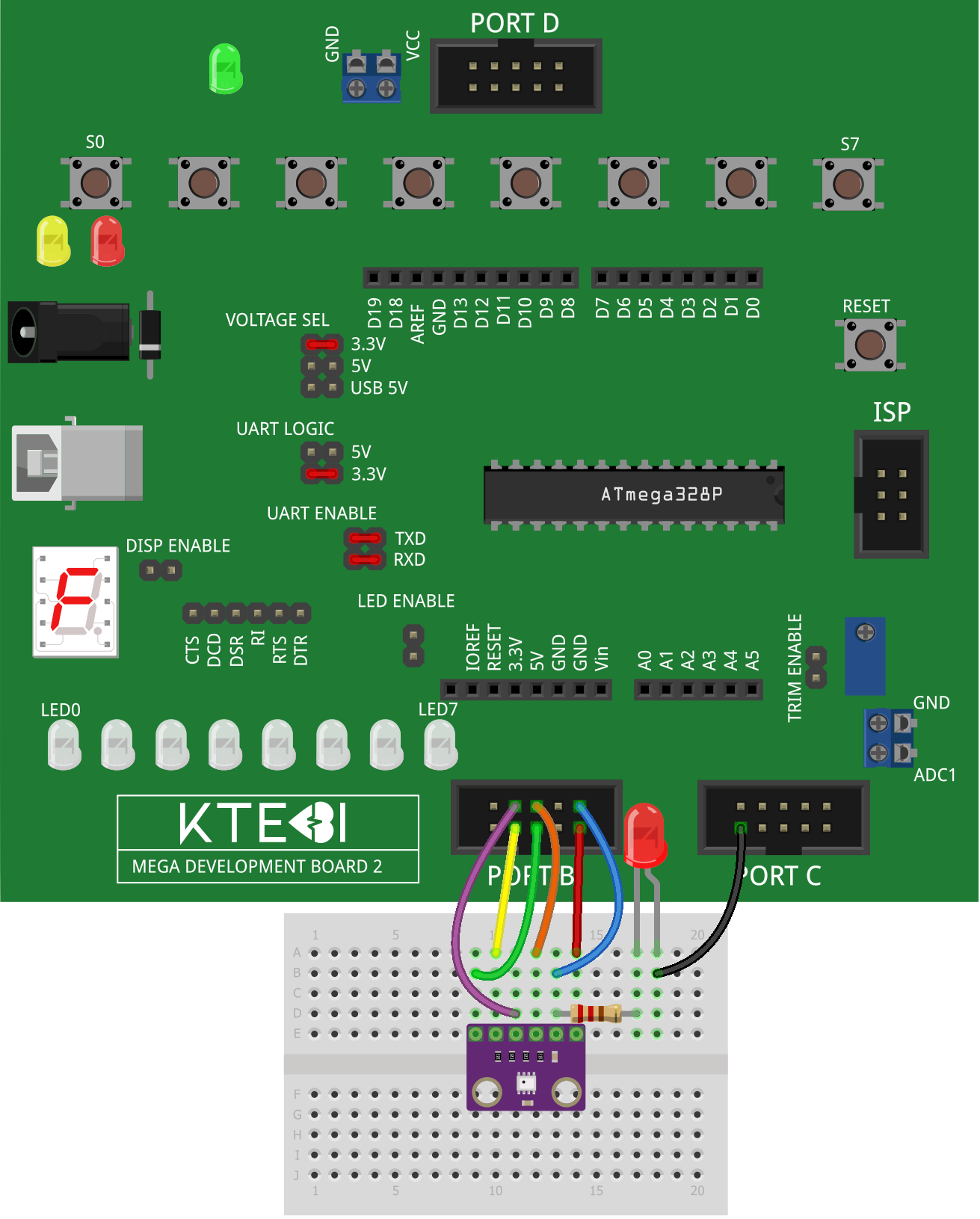
The SPI interface is activated by grounding (connecting to GND) the CSB pin. According to the schematic in Fig. 3, a pull-up resistor is connected to this pin. We connect the CSB pin to an MCU output pin (in our case PB2), which is driven to logic low right at the beginning of program execution. This ensures that the SPI interface is activated. If the voltage level on the CSB pin subsequently changes to logic 1, the communication interface remains locked in SPI mode. The SPI interface supports both mode '00' (CPOL=0, CPHA=0) and mode '11' (CPOL=1, CPHA=1). Furthermore, both 4-wire and 3-wire SPI communication modes can be used. The 3-wire interface must be enabled in the config register (bit spi3w_en=1). The maximum achievable data transfer rate via SPI is 10 MHz. In our case, we will use a standard 4-wire interface and a clock frequency of 1 MHz.
When the sensor operates in SPI mode, only 7-bit register addresses are used. The most significant bit (MSB) of the address byte is replaced by the RW bit indicating read/write: RW=1 for read operations and RW=0 for write operations.
For example, address 0xF7 from the register map is accessed via SPI as 0x77. To write to this address (RW=MSB=0), the value 0x77 is transmitted over SPI. To read from this address (RW=MSB=1), the value 0xF7 is transmitted.
Writing via SPI
A write operation begins by driving the CSB pin to logic 0 (CSB=0) and transmitting a byte pair: the target register address (Control byte), followed by the payload data (Data byte). The Control byte consists of the 7-bit register address (address without bit 7) and the write indicator (bit 7=RW=0). Multiple registers can be written in a single burst without toggling the CSB pin. The write sequence is terminated by driving the CSB pin back to logic 1. The SPI write protocol is illustrated in Fig. 1.

Reading via SPI
A read operation begins by driving the CSB pin to logic 0 (CSB=0) and transmitting a single Control byte (register address). The Control byte consists of the 7-bit register address (address without bit 7) and the read indicator (bit 7=RW=1). After transmitting the control byte, the requested data is shifted out on the SDO (MISO) line to the MCU. During read operations, the register address auto-increments automatically, meaning subsequent registers can be read consecutively without retransmitting the control byte (Control byte). The SPI read protocol is illustrated in Fig. 2.

2. Equipment Used
- Hardware
- Mega Development Board 2 (MDB2)
- BMP280 temperature sensor on breakout PCB
- PC
- Software
- MATLAB
- Microchip Studio
3. Schematic Diagram
4. Assignment Tasks
- Connect the BMP280 sensor to the MDB2 development board according to the connection diagram (Fig. 3). Use an external DC power adapter. The jumper positions on the MDB2 are highlighted in red—the sensor power supply voltage must be set to 3.3 V! Selecting 5 V can permanently damage the sensor!
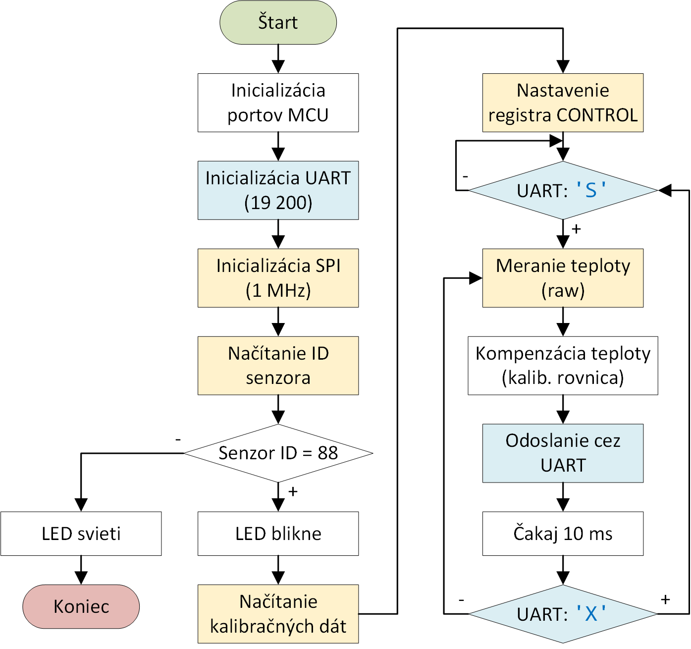
- Write an MCU firmware program in C to acquire data from the BMP280 sensor via a 4-wire SPI interface and stream the measured temperature readings to the PC over UART. Implement the following parameters and functionality in the code:
- SPI clock frequency: 1 MHz,
- Sample temperature data from the sensor and transmit them to the PC every 100 ms,
- Configure the UART baud rate to 19,200 Baud,
- Begin streaming samples to the PC only after receiving the character 'S', and stop transmission upon receiving the character 'X'. Use the UART receive interrupt to detect incoming control characters,
- Structure the program according to the flowchart below:
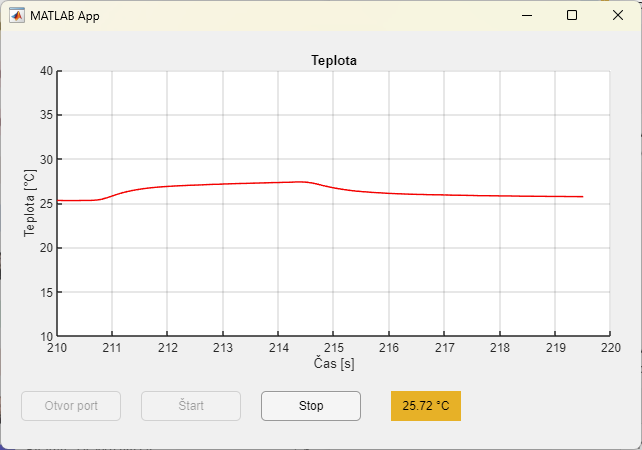
- Develop a graphical user interface application in MATLAB App Designer that displays the real-time temperature in °C and plots its trend over time as shown in Fig. 5. The application must feature:
- An axes plot for rendering real-time temperature over time,
- A text field displaying the current temperature,
- Control pushbuttons: 'Open Port', 'Start', and 'Stop'.
- Evaluate the laboratory exercise. Focus on the following points:
- Writing the MCU firmware and resolving implementation bottlenecks,
- Developing the companion MATLAB GUI application.