


Temperature Measurement Using an I2C Interface Sensor
1. Theoretical Introduction
The BMP280 integrated circuit from Bosch is a digital barometric pressure sensor that also enables temperature measurement. It measures pressure across a range from 30 kPa to 110 kPa. Its relative accuracy is ±12 Pa, which is equivalent to an altitude variation of ±1 m, allowing the sensor to be utilized as an altimeter. The sensor measures temperature in the range of -40 °C to +85 °C, achieving its highest temperature measurement accuracy within (0 ÷ +65) °C at ±1 °C (around 25 °C, accuracy is ±0.5 °C). The maximum output data resolution is 0.16 Pa for pressure and 0.01 °C for temperature. The device draws only 2.7 µA at a 1 Hz sampling frequency. It can be supplied with a voltage ranging from 1.71 V to 3.6 V. The sensor communicates via an I2C or SPI interface.
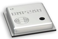
In this laboratory exercise, the BMP280 sensor mounted on a breakout PCB (Fig. 2) will be used to allow insertion into a solderless breadboard. In addition to the sensor IC, the breakout board includes the necessary passive components.

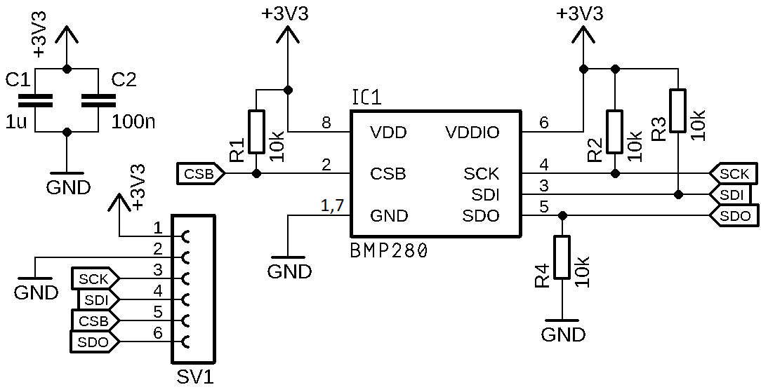
The schematic diagram of the BMP280 along with discrete components is shown in Fig. 3. Capacitors C1 and C2 serve as decoupling filters for power supply noise. Resistor R1 acts as a pull-up resistor to enable the I2C interface. Similarly, resistors R2 and R3 function as pull-up resistors for the I2C communication lines—SDA and SCL. Resistor R4 acts as a pull-down resistor and configures the default I2C address of the sensor when I2C communication is used. The default 7-bit sensor address is 0x76. If the SDO pin is tied to +3.3 V, the I2C address changes to 0x77.
The pinout of the breakout board is shown in Fig. 4.
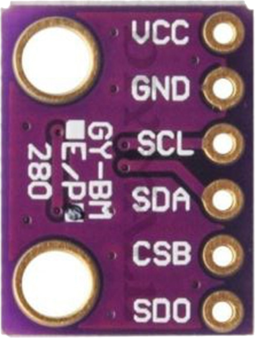
| # | Pin Name (I2C) | Pin Name (BMP280) | Pin Name (SPI) | Function |
|---|---|---|---|---|
| 1 | VCC | VDD | VCC | Power supply 1.71 V ÷ 3.6 V |
| 2 | GND | GND | GND | Ground |
| 3 | SCL | SCK | SCK | Clock signal (I2C + SPI) |
| 4 | SDA | SDI | MOSI | Data line (I2C), data input (SPI) |
| 5 | CSB | CSB | CSB/CS | I2C/SPI mode select, chip select (SPI) |
| 6 | SDO | SDO | MISO | Data output (SPI) |
The sensor supports both I2C and SPI serial interfaces. Interface selection is carried out via the CSB pin. When the CSB pin is tied to VDDIO/supply (+3.3 V), the I2C interface is enabled. Connecting the CSB pin to ground activates the SPI interface. From the schematic in Fig. 3, it can be seen that the CSB pin is tied to supply through a pull-up resistor, meaning that the I2C communication interface remains active even when the CSB pin is left unconnected.
BMP280 Sensor Register Map
Measured pressure and temperature values, as well as sensor configuration parameters, are stored in memory locations referred to as registers. The register map is fundamental for working with the device. It details the names, memory addresses, and bit-level layout of all registers. The register map is shown in Fig. 5. For example, the sensor identification register (ID) is located at address 0xD0. This register holds the value 0x58 (88D), which should be read back over I2C or SPI to verify that the communication interface is functional and properly configured.

The following sections cover only the registers directly relevant to the temperature measurement objective of this laboratory exercise.
Register calib
The sensor is calibrated during manufacturing, and its calibration coefficients are programmed into non-volatile ROM. The calib registers hold the calibration coefficients for temperature and pressure. The registers storing the temperature calibration coefficients are listed in the table below.
| Register Name | Register Address (From – To) | Register Content | Data Type |
|---|---|---|---|
| calib00 | 0x88 – 0x89 | dig_T1 | Uint16 |
| calib01 | 0x8A – 0x8B | dig_T2 | Int16 |
| calib02 | 0x8C – 0x8D | dig_T3 | Int16 |
Register ctrl_meas
This register sets the oversampling and data resolution for temperature and pressure, as well as the sensor operating mode.
| bit 7 | bit 6 | bit 5 | bit 4 | bit 3 | bit 2 | bit 1 | bit 0 |
|---|---|---|---|---|---|---|---|
| osrs_t[2:0] | osrs_p[2:0] | mode[1:0] | |||||
| osrs_t[2:0] | Controls oversampling of temperature data and determines sample resolution – Table 2 |
| osrs_p[2:0] | Controls oversampling of pressure data and determines sample resolution. |
| mode[1:0] | Controls the sensor power/operating mode (Table 3). |
| osrs_t[2:0] | Temperature Oversampling | Typical Temperature Resolution |
|---|---|---|
| 000 | Skipped (output 0x800000) | - |
| 001 | × 1 | 16 bit / 0.0050 °C |
| 010 | × 2 | 17 bit / 0.0025 °C |
| 011 | × 4 | 18 bit / 0.0012 °C |
| 100 | × 8 | 19 bit / 0.0006 °C |
| 101, 110, 111 | × 16 | 20 bit / 0.0003 °C |
| mode[1:0] | Mode |
|---|---|
| 00 | Sleep mode |
| 01, 10 | Forced mode |
| 11 | Normal mode |
Sleep mode is the default power state upon power-up. In this mode, no measurements are performed and power consumption is minimal. All internal registers remain accessible.
Forced mode performs a single measurement of temperature and pressure. Once the measurement cycle completes, the sensor returns to Sleep mode, and the conversion results are placed in the respective data registers. A subsequent measurement requires configuring Forced mode again in the ctrl_meas register. This mode is recommended for applications that do not require high sampling rates or when synchronization with an external MCU is required.
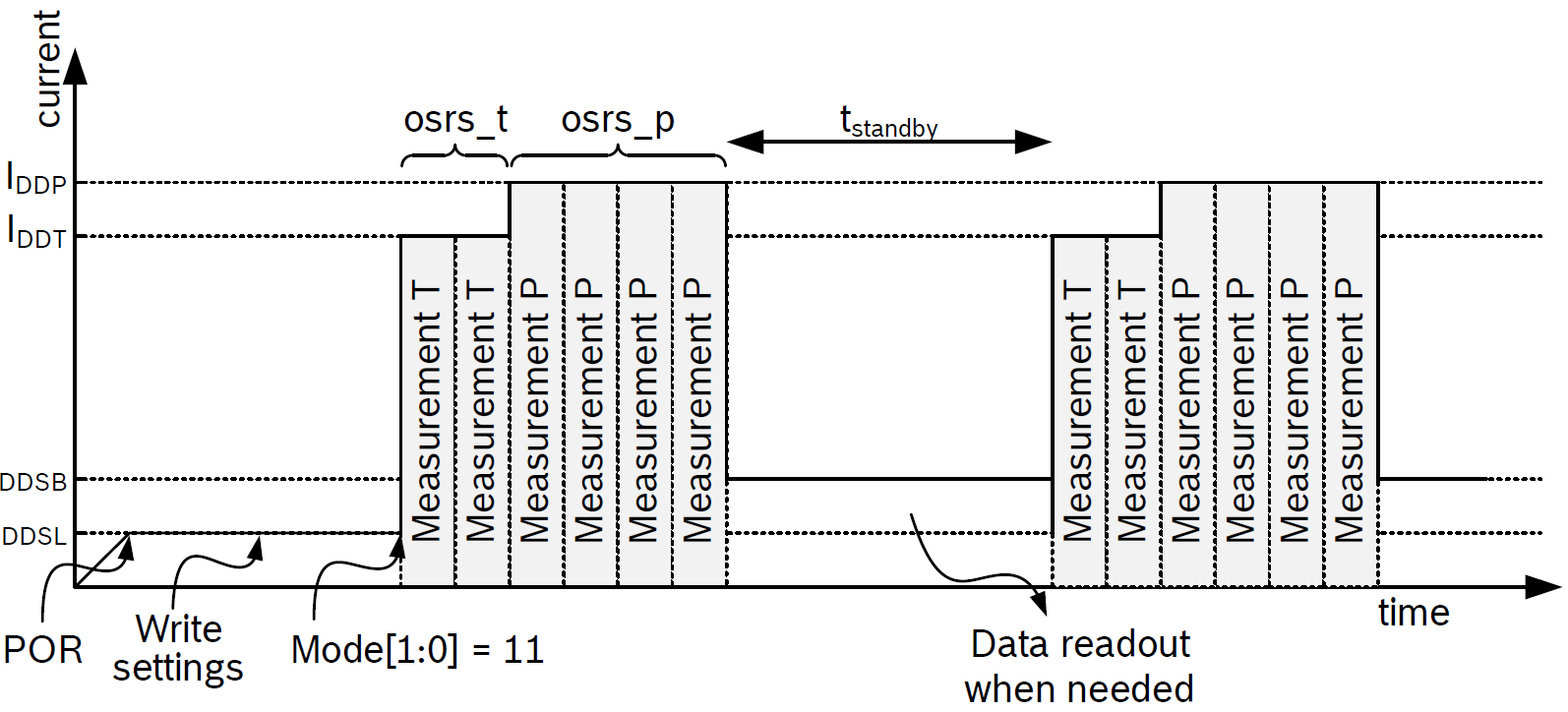
Normal mode provides continuous cycling between active measurement and an inactive standby period (Fig. 6). The duration of this standby interval is denoted as tstandby. This standby time is configured via the config register.
Register config
This register sets the rate/standby time, filter coefficient, and SPI wire configuration.
| bit 7 | bit 6 | bit 5 | bit 4 | bit 3 | bit 2 | bit 1 | bit 0 |
|---|---|---|---|---|---|---|---|
| t_sb[2:0] | filter[2:0] | spi3w_en[0] | |||||
| t_sb[2:0] | Controls standby duration tstandby. (Table 4) |
| filter[2:0] | Sets the time constant of the IIR filter. |
| spi3w_en[0] | Enables 3-wire SPI interface mode. |
| t_sb[2:0] | tstandby [ms] |
|---|---|
| 000 | 0.5 |
| 001 | 62.5 |
| 010 | 125 |
| 011 | 250 |
| 100 | 500 |
| 101 | 1000 |
| 110 | 2000 |
| 111 | 4000 |
The internal IIR filter is primarily intended for filtering pressure data; therefore, tuning the IIR filter parameters is not required for this exercise.
The SPI interface can operate in two modes: 4-wire and 3-wire. Setting the spi3w_en bit enables 3-wire mode, in which the SDI pin acts as a bidirectional data line.
Registers temp_msb, temp_lsb, temp_xlsb
These registers hold the raw measured temperature data directly from the internal ADC. Combining these registers forms a 20-bit value. To convert this raw reading into degrees Celsius, the compensation formula specified in the datasheet must be evaluated.
| bit 7 | bit 6 | bit 5 | bit 4 | bit 3 | bit 2 | bit 1 | bit 0 |
|---|---|---|---|---|---|---|---|
| temp_msb[7:0] | |||||||
| bit 7 | bit 6 | bit 5 | bit 4 | bit 3 | bit 2 | bit 1 | bit 0 |
|---|---|---|---|---|---|---|---|
| temp_lsb[7:0] | |||||||
| bit 7 | bit 6 | bit 5 | bit 4 | bit 3 | bit 2 | bit 1 | bit 0 |
|---|---|---|---|---|---|---|---|
| temp_xlsb[7:4] | 0 | 0 | 0 | 0 | |||
The following C function calculates the temperature in [°C] (T) from the raw ADC value (adc_T) by substituting the calibration coefficients (dig_T1, dig_T2, dig_T3) into the compensation formula.
int32_t bmp280_compensate_T_int32(int32_t adc_T)
{
int32_t var1, var2, T, t_fine;
var1 = ((((adc_T>>3) - ((int32_t)dig_T1<<1))) * ((int32_t)dig_T2)) >> 11;
var2 = (((((adc_T>>4) - ((int32_t)dig_T1)) * ((adc_T>>4) - ((int32_t)dig_T1))) >> 12) * ((int32_t)dig_T3)) >> 14;
t_fine = var1 + var2;
T = (t_fine * 5 + 128) >> 8;
return T;
}
I2C Communication
When the CSB pin on the breakout board is left unconnected (pulled high via on-board pull-up), the I2C interface is automatically enabled on power-up. Three I2C bus speeds are supported: Standard mode (100 kbit/s), Fast mode (400 kbit/s), and High Speed mode (3.4 Mbit/s). The 7-bit slave address is 0x76 or 0x77 depending on the SDO pin connection. In our circuit, the address is 0x76 because SDO is grounded in Fig. 3. The hexadecimal value 0x76 corresponds to the 7-bit binary value 0b1110110.
Writing via I2C
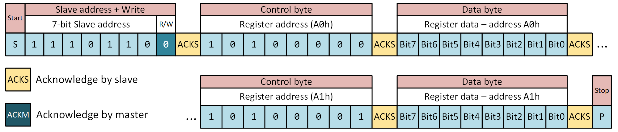
A write transaction begins by transmitting the slave address (Slave address) with the write bit cleared (R/W = 0), i.e., 0b11101100 (0xEC). Next, the target register address (Control byte) is transmitted, followed by the payload data (Data byte). Multiple registers can be written sequentially without retransmitting the slave address. The transfer is completed with a STOP condition. Multi-byte writing is shown in Fig. 7.
Reading via I2C
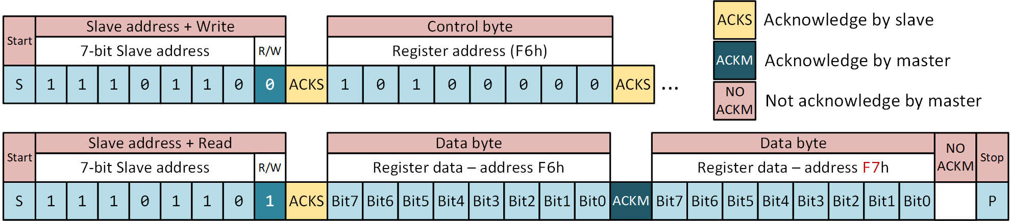
To read from sensor registers, the master first sends the slave address with write mode, i.e., 0b11101100 (0xEC), followed by the address of the target register to read (Control byte). Then, a STOP condition or a repeated START condition must be generated. Next, the slave address is re-sent with read mode enabled (R/W = 1), i.e., 0b11101101 (0xED). Following this byte, the sensor returns the data stored at the requested register address. During read operations, the internal register pointer auto-increments, allowing consecutive registers to be read continuously without retransmitting the address. Reading continues until the master issues a NACK and a STOP condition. Fig. 8 demonstrates reading register 0xF6 followed by register 0xF7, yielding 2 bytes in total.
2. Equipment Used
- Hardware
- Mega Development Board 2 (MDB2)
- BMP280 temperature sensor on breakout PCB
- PC
- Software
- MATLAB
- Microchip Studio
3. Schematic Diagram
4. Assignment Tasks
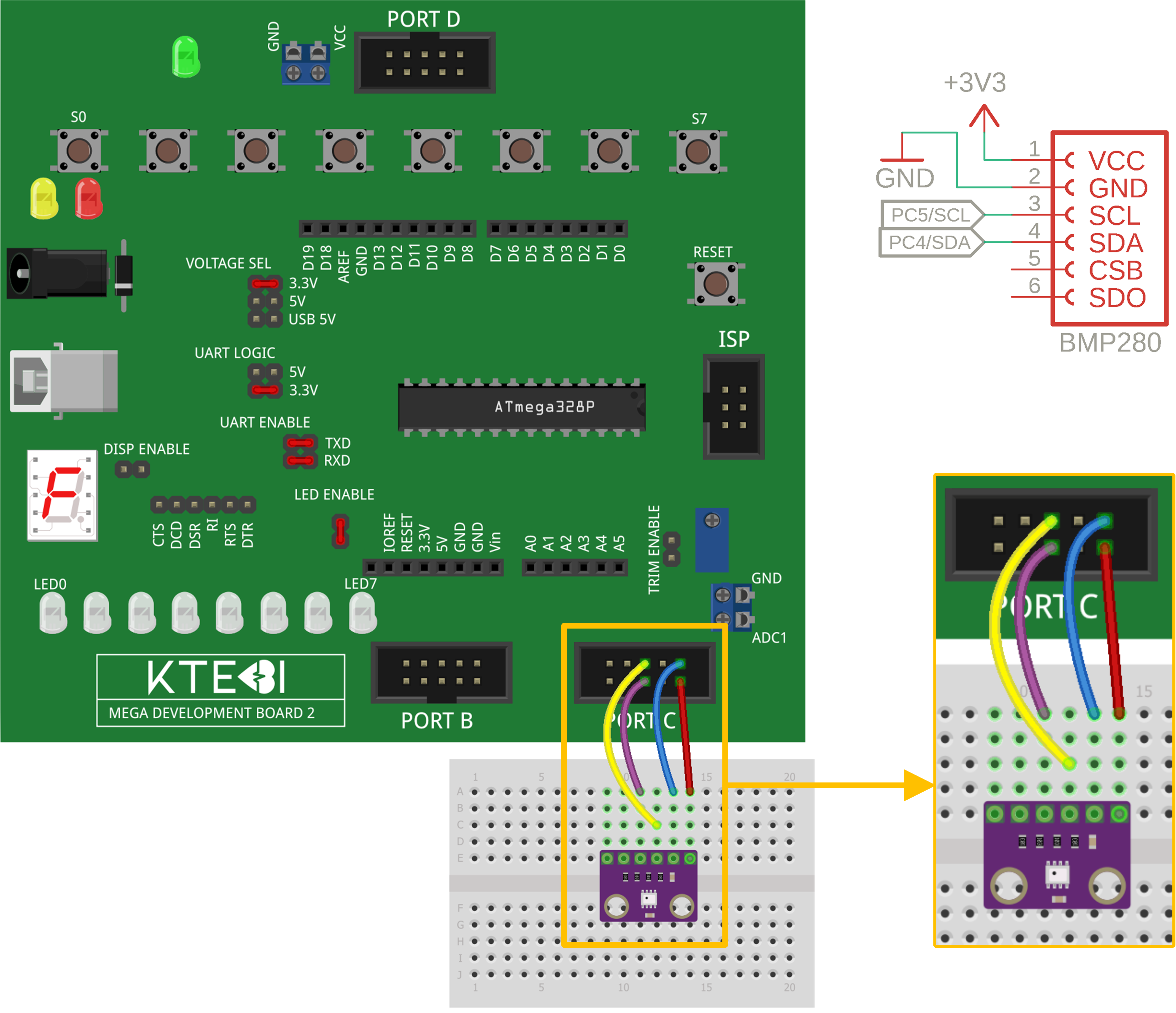
- Connect the BMP280 sensor to the MDB2 development board according to the wiring schematic (Fig. 9). Use an external DC power adapter. The jumper positions on the MDB2 board are highlighted in red—the sensor power supply voltage must be set to 3.3 V! Selecting 5 V can permanently damage the sensor!
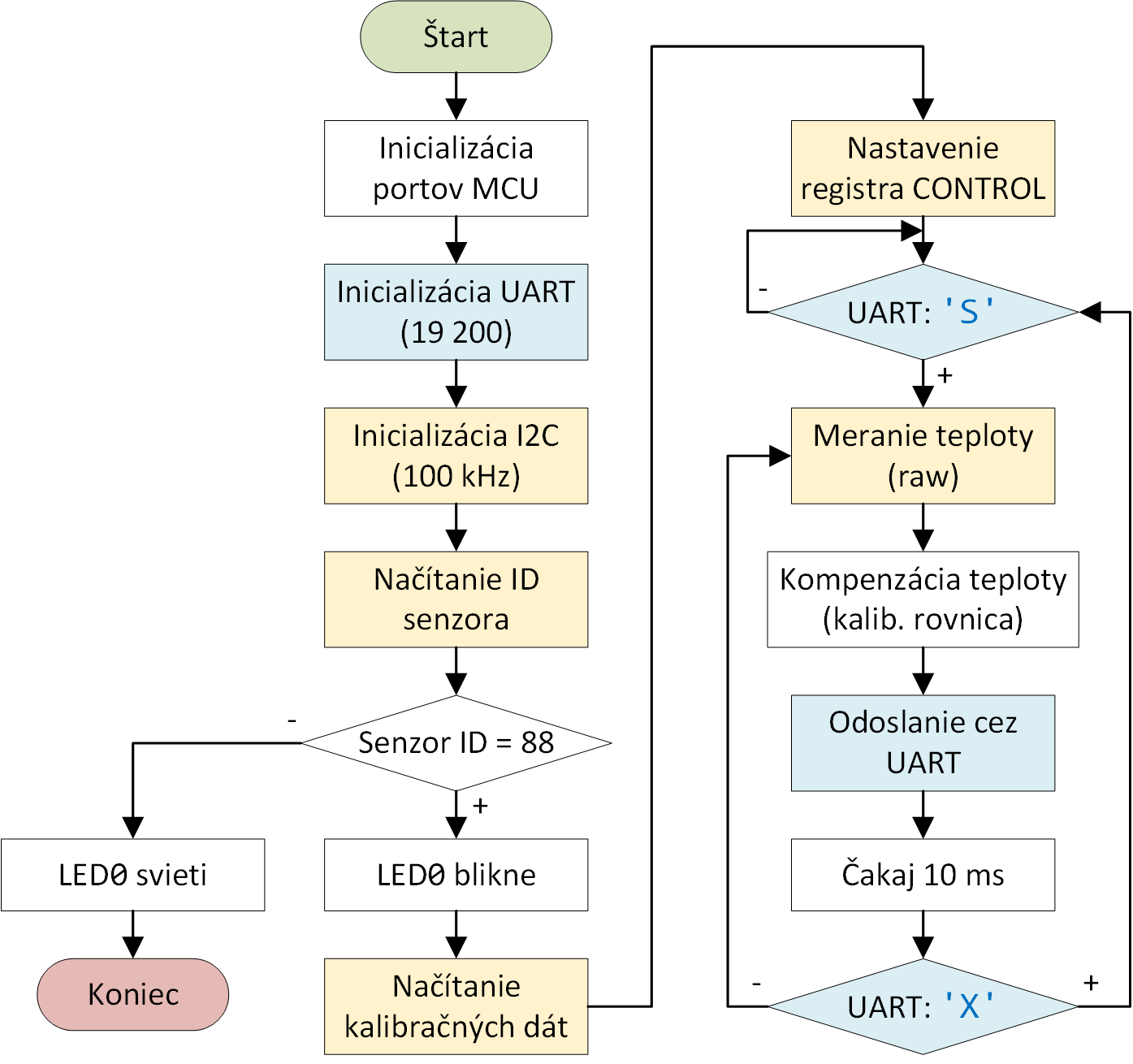
- Write an MCU firmware program in C to read data from the BMP280 sensor via the I2C interface and stream the temperature readings to the PC over UART. Implement the following specifications and functions in the code:
- I2C bus clock frequency: 100 kHz,
- Sample temperature data from the sensor and transmit them to the PC every 100 ms,
- Set the UART baud rate to 19,200 Baud,
- Begin streaming samples to the PC only after receiving the character 'S', and stop transmission upon receiving the character 'X'. Use the UART receive interrupt to detect incoming control characters,
- Structure the program according to the flowchart below:
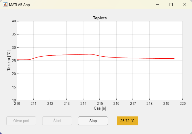
- Develop a graphical user interface application in MATLAB App Designer that displays the real-time temperature in °C and plots its trend over time as shown in Fig. 11. The application must feature:
- An axes component for plotting real-time temperature over time,
- A numeric display or edit field for the current temperature,
- Control pushbuttons: 'Open Port', 'Start', and 'Stop'.
- Evaluate the laboratory assignment. Focus on the following points:
- Writing the MCU firmware and resolving implementation bottlenecks,
- Developing the companion MATLAB GUI application.
Downloads
twimaster.htwimaster.c