


Analog-to-Digital Converter (ADC) in AVR Microcontrollers
Most physical phenomena in the real world (such as temperature, barometric pressure, mechanical strain, optical intensity, and biopotentials) are continuous, analog quantities. To process, analyze, and manipulate these signals using a digital microcontroller, they must be converted into a sequence of discrete numerical values. This critical interface is realized by an Analog-to-Digital Converter (ADC).
The ATmega328P microcontroller incorporates an on-chip 10-bit ADC based on the Successive Approximation Register (SAR) architecture. The converter core is coupled to an analog multiplexer (ADMUX), allowing the acquisition of signals from multiple external pins (ADC0 through ADC7 depending on package footprint) as well as internal signal sources (such as the internal bandgap reference or the integrated chip temperature sensor).
Core operating principles and parameters vital for configuring the ADC:
- Resolution: The converter features 10-bit resolution, discretizing the analog input voltage span into 210 = 1024 quantization levels (ranging from code 0 to 1023). The resulting 10-bit conversion output is stored across the 16-bit register pair ADCH:ADCL.
- Reference Voltage (VREF): Sets the full-scale ceiling of the measurable input range corresponding to maximum code ($1023$). Selectable options include the analog supply rail AVCC, an external reference applied to the AREF pin, or an internal calibrated 1.1 V voltage source. The quantization step size (LSB voltage weight) is evaluated as: LSB = VREF/1024
- ADC Clock Frequency: The successive approximation circuitry requires an input clock frequency between 50 kHz and 200 kHz to achieve full 10-bit accuracy. This clock is scaled down from the primary MCU system clock via a dedicated prescaler offering division factors of 2, 4, 8, 16, 32, 64, or 128.
- Conversion Modes: The ADC operates in either Single Conversion mode (where each sampling cycle is triggered manually via software register write) or Free Running / Auto Triggered mode (where a new acquisition begins automatically upon completion of the previous cycle or is synchronized to peripheral timer/counter events).
The completion of an analog-to-digital conversion is flagged by dedicated hardware status registers. Furthermore, the peripheral can assert an ADC Conversion Complete Interrupt, enabling non-blocking, interrupt-driven biosignal and sensor data acquisition in the background.
Important Registers
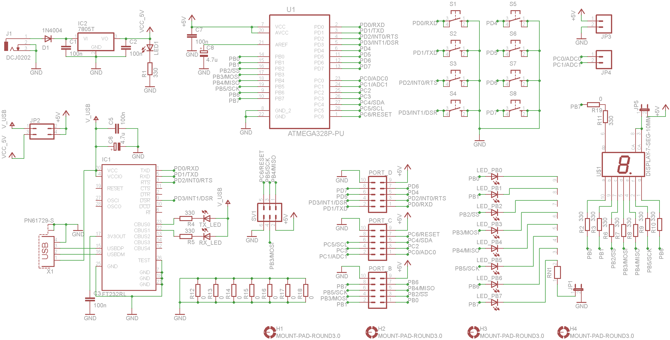
This section describes several registers associated with the internal ADC (Analog-to-Digital Converter) that are used in the examples below.
ADMUX – ADC Multiplexer Selection Register, used to configure the ADC voltage reference and select the analog input channel connected to the ADC.
- Bits REFS1 and REFS0 select the ADC voltage reference according to the table below. If you are using the Mega Development Board for testing, use the configuration REFS1=0 and REFS0=1. In the schematic of the Mega Development Board, the AVCC pin is connected to VCC = 5V. The reference voltage is therefore AVCC = 5V.


- The ADLAR bit affects the presentation of the ADC conversion result in the 16-bit ADC Data Register (described below). If ADLAR=1, the result is left-adjusted; otherwise, the result is right-adjusted.
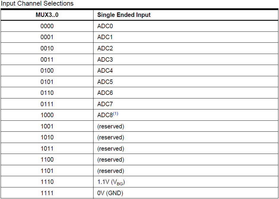
- Bits MUX3 through MUX0 select the analog input channel (ADC0 through ADC8) routed to the ADC converter. The Mega Development Board exposes channels ADC0 and ADC1 on its terminal block.
ADCSRA – ADC Control and Status Register A.

- The ADEN bit enables/disables the ADC. Setting ADEN=1 enables the ADC. Turning the ADC off during a conversion (ADEN=0) terminates the ongoing conversion.
- The ADSC bit starts an ADC conversion. Writing ADSC=1 initiates each single conversion. Once the conversion is complete, this bit is automatically cleared to zero (ADSC=0). Writing ADSC=0 has no effect.
- The ADIF bit is set (ADIF=1) when an ADC conversion is completed and the data registers are updated. ADIF is cleared automatically (by hardware) when executing the corresponding ADC Conversion Complete Interrupt vector, or by software by writing a logic one to the flag.
- The ADIE bit enables the ADC Conversion Complete Interrupt.
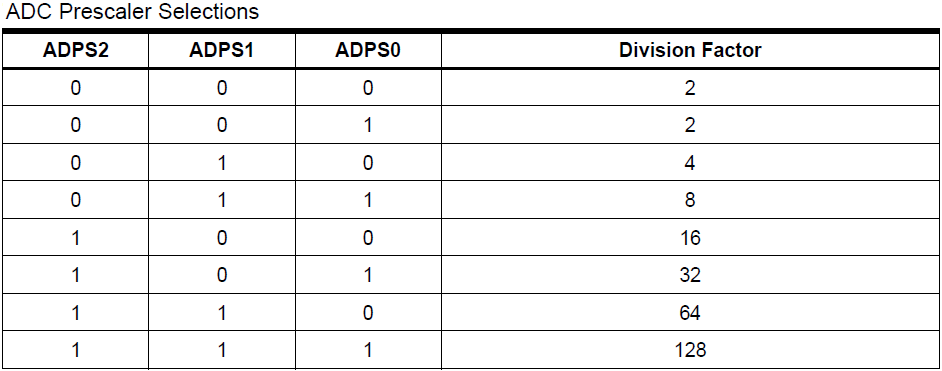
- Bits ADPS2 through ADPS0 configure the ADC clock prescaler (Division Factor) relative to the MCU system clock. The settings are shown in the following table. The input clock frequency to the ADC must be between 50 kHz - 200 kHz to achieve maximum 10-bit resolution. Setting the ADC prescaler therefore depends on the MCU system clock (the ATmega328P uses an 8 MHz internal oscillator).
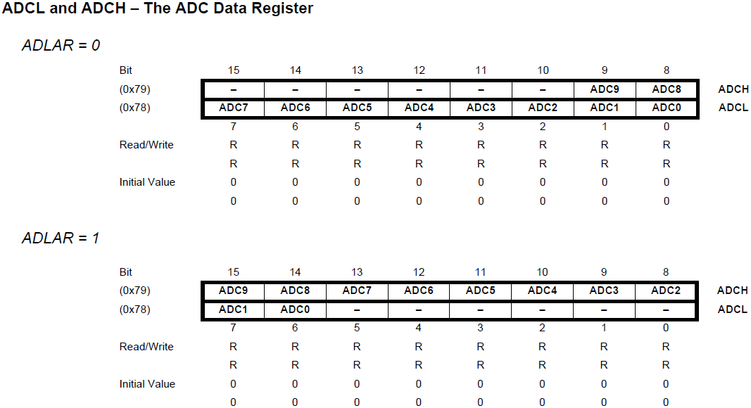
ADC – 16-bit Data Register holding the result of the conversion. The register consists of two 8-bit registers: ADCH (High byte) and ADCL (Low byte). Depending on the setting of the ADLAR bit in the ADMUX register, the conversion result is either right-adjusted or left-adjusted.
The ADC conversion result (contents of the ADC register) for 10-bit resolution is calculated according to the formula:

Example 1
This example describes using the internal 10-bit ADC to digitize an analog voltage signal applied to the ADC input pin ADC0 (PORTC0). The ADC reference voltage is 5V. When 0V is applied to the ADC0 input, the number 0 lights up on the display, and when 5V is applied, the number 5 lights up. A voltage of 0V corresponds to the minimum digital value of 0, and 5V corresponds to the maximum digital value of 1023. Because the ADC input may pick up slight electrical noise, the display shows 0 whenever the digital reading is below 100. The number 5 is displayed when the digital reading is greater than 950. If the reading falls outside these ranges, the display remains off.
#include <avr/io.h>
void ADC_Init()//inicializacia AD prevodnika
{
ADMUX|=(1<<REFS0);//referencia na AVCC pine
//v scheme su piny VCC a AVCC prepojene -> referencia AD prevodnika = 5V
//digitalizujeme kanal ADC0 - prednastavena hodnota v registri ADMUX
ADCSRA|=(1<<ADPS2)|(1<<ADPS1);//predelicka 64 -> 125kHz
ADCSRA|=(1<<ADEN);//povolenie AD prevodnika
}
uint16_t StartPrevodu()//funkcia s navratovou hodnotou typu uint16
{
ADCSRA|=(1<<ADSC);//start prevodu
while ((ADCSRA&(1<<ADIF))==0) ; //caka na dokoncenie prevodu
ADCSRA|=(1<<ADIF);//nulovanie dokoncenia prevodu zapisom log.1
return ADC;//vysledok prevodu je v registri ADC
}
void ZhasniDisplej()
{
PORTB=255;//zhasne displej (vsetky segmenty)
}
void RozsvietNulu()
{
PORTB=(1<<PORTB6);//zhasne segment G
}
void RozsvietPatku()
{
PORTB=(1<<PORTB1)|(1<<PORTB4);//zhasne segmenty B a E
}
int main(void)
{
DDRB=255;//PORTB ako vystupny (pripojeny displej)
ZhasniDisplej();
ADC_Init();//inicializacia AD prevodnika
while (1)
{
uint16_t hodnota=StartPrevodu();
if (hodnota<100)
RozsvietNulu();
else
{
if (hodnota>950)
RozsvietPatku();
else
ZhasniDisplej();
}
}
}
Example 2
In the following example, an analog signal applied to the ADC0 pin is digitized at a sampling frequency of fs = 100 Hz (Ts = 10 ms). The digital samples are transmitted to a PC over the USART interface (Baud Rate = 19,200). This example is comprehensive, as it incorporates a timer, an interrupt, and the USART interface, all introduced in preceding lessons.
#include <avr/io.h>
#include <avr/interrupt.h>
#define RTS PIND2
void ADC_Init()//inicializacia AD prevodnika
{
ADMUX|=(1<<REFS0);//referencia na AVCC pine
//v scheme su piny VCC a AVCC prepojene -> referencia AD prevodnika = 5V
//digitalizujeme kanal ADC0 - prednastavena hodnota v registri ADMUX
ADCSRA|=(1<<ADPS2)|(1<<ADPS1);//predelicka 64 -> 125kHz
ADCSRA|=(1<<ADEN);//povolenie AD prevodnika
}
void Timer1_Init()//inicializacia 16-bit casovaca (TIMER1)
{
TCCR1B|=(1<<CS11);//zapnutie casovaca predelicka 8 -> fCPU=8MHz-> f_casovac=1MHz -> T_casovac=1us
OCR1A=10000;//10000x1us=10ms->fvz=100 Hz
TCCR1B|=(1<<WGM12); //automaticke nulovanie TCNT1 pri dosiahnuti hodnoty v OCR1A
TIMSK1=(1<<OCIE1A);//zapnutie prerusenia casovaca (TIMER1_COMPA_vect)
}
void USART_Init()
{
// Nastavenie USART-8 datovych bitov,jeden stop bit,ziadna parita
// - uvedene parametre su vychodiskove hodnoty registrov,
// preto nie je potrebne nastavovat
UBRR0=25; //nastavena rychlost 19200 Baud (z datasheetu) pri f_MCU=8MHz
UCSR0B|=(1<<TXEN0); //zapnutie vysielaca
}
void USART_send(unsigned char bajt)
{
while ( !( UCSR0A & (1<<UDRE0)) ) ; //pocka na vyprazdnenie buffera
UDR0 = bajt; //odoslanie bajtu cez USART
}
uint16_t StartPrevodu()//funkcia s navratovou hodnotou typu uint16
{
ADCSRA|=(1<<ADSC);//start prevodu
while ((ADCSRA&(1<<ADIF))==0) ; //caka na dokoncenie prevodu
ADCSRA|=(1<<ADIF);//nulovanie dokoncenia prevodu zapisom log.1
return ADC;//vysledok prevodu je v registri ADC
}
ISR(TIMER1_COMPA_vect) //obsluha prerusenia casovaca TIMER1
{
//prerusenie sa spusta kazdych 10ms
if (! (PIND&(1<<RTS)))//ak je linka RTS na log.0
{
uint16_t digi_hodnota=StartPrevodu();
//digi_hodnota = 16 bit = 2 bajty
USART_send(digi_hodnota);//odosle dolny bajt
USART_send(digi_hodnota>>8);//odosle horny bajt
}
}
int main(void)
{
DDRD&=~(1<<RTS);//pin RTS (PIND2) ako vstupny
ADC_Init();//inicializacia AD prevodnika
Timer1_Init();//inicializacia casovaca TIMER1 (16 bit)
USART_Init();//inicializacia USART
sei();//globalne povolenie preruseni
while (1)
{
}
}