


Controlling a 4-Digit 7-Segment Display Using a Shift Register
1. Introduction
Shift registers are an important element in digital circuits. Their primary function is to "shift" data (binary values) from input(s) to output(s) depending on additional control signals (e.g., a clock signal). Shift registers belong to the family of sequential digital circuits, most commonly composed of D or RS flip-flops. Based on their operation, shift registers can be divided into four basic categories:
- SIPO (Serial In – Parallel Out),
- PISO (Parallel In – Serial Out),
- SISO (Serial In – Serial Out),
- PIPO (Parallel In – Parallel Out).
In this laboratory exercise, we will use a SIPO shift register, which is used to expand the number of outputs from a single serial input. This type of register is useful when a microcontroller (MCU) lacks the required number of pins to drive components such as LEDs. Let us look at a specific example: the ATmega328P MCU features 23 usable pins (pin PC7 is unavailable), allowing up to 23 LEDs to be connected in theory. This is only theoretical because the maximum recommended total current across all outputs is 200 mA; exceeding this limit can cause overheating and MCU instability. Connecting more than 23 LEDs can be achieved using a SIPO shift register, which expands the available outputs while preventing overcurrent conditions on the MCU. We will use the 74HC595 shift register in this lab. Its functional block diagram is shown in Fig. 1.
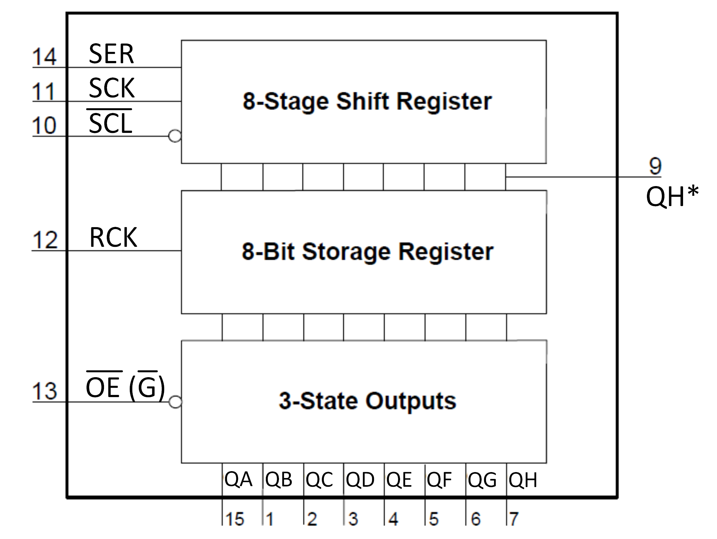
Serial data is fed into the SER input. The parallel output consists of pins QA – QH. The serial-to-parallel conversion process is driven by signals on pins SCK, SCL, RCK, and OE. The following table describes the function of each pin.
| Pin Label | Description | Function |
|---|---|---|
| SER | Serial Data Input | Data input |
| SCK | Shift Register Clock Input | Clock signal for input data |
| SCL | Master Reset Input | Clears the Shift Register |
| RCK | Storage Register Clock Input | Clock signal for transferring data from the Shift Register to the Storage Register |
| OE | Output Enable | Enables outputs QA–QH |
| QA - QH | Parallel Data Output | Parallel register outputs |
| QH* | Serial Data Output | Serial output used for cascading additional shift registers. |
Binary data is shifted from the SER input to the outputs (QA - QH) according to the timing diagram in Fig. 2.
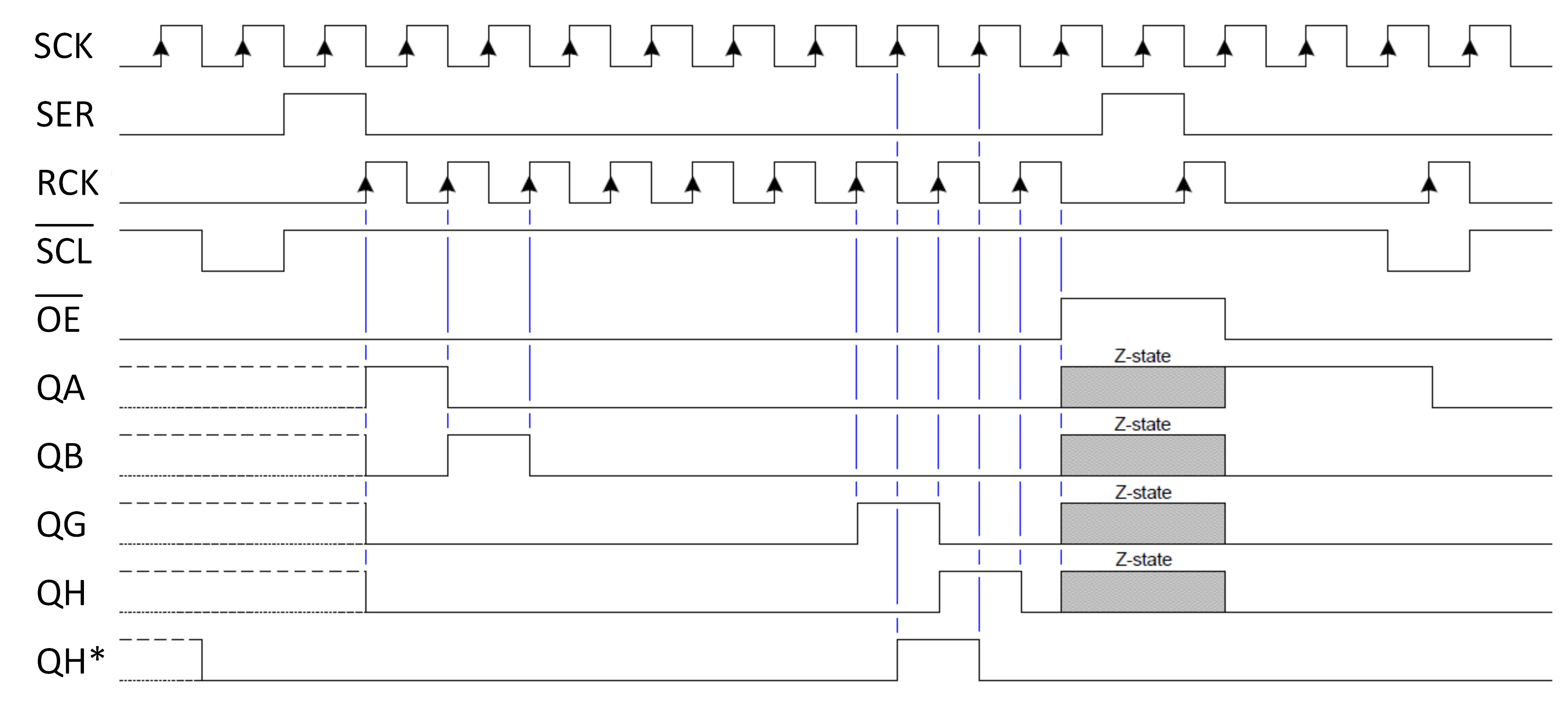
As shown in Fig. 2, generating 8 outputs (QA - QH) from a single data input (SER) requires 5 MCU pins (SCK, SER, RCK, SCL, and OE). An advantage of shift registers is that they can be cascaded by connecting the QH* serial output of one register to the SER input of the next. Cascading does not require additional MCU pins, allowing virtually unlimited registers to be linked. For example, controlling 64 LEDs would require cascading eight 74HC595 registers while still using only 5 MCU pins.
The main objective of this lab is to display digits on a 4-digit 7-segment display. Since the display requires multiple control lines, two 74HC595 shift registers—labeled U2 and U3—are used. The display is integrated into an Arduino add-on board: the Multi-Function Shield. The schematic of the display and its interface to the shift registers is shown in Fig. 3. Pin SCL is tied directly to +5V and pin G (OE) to GND, reducing the required MCU pins from 5 down to 3.
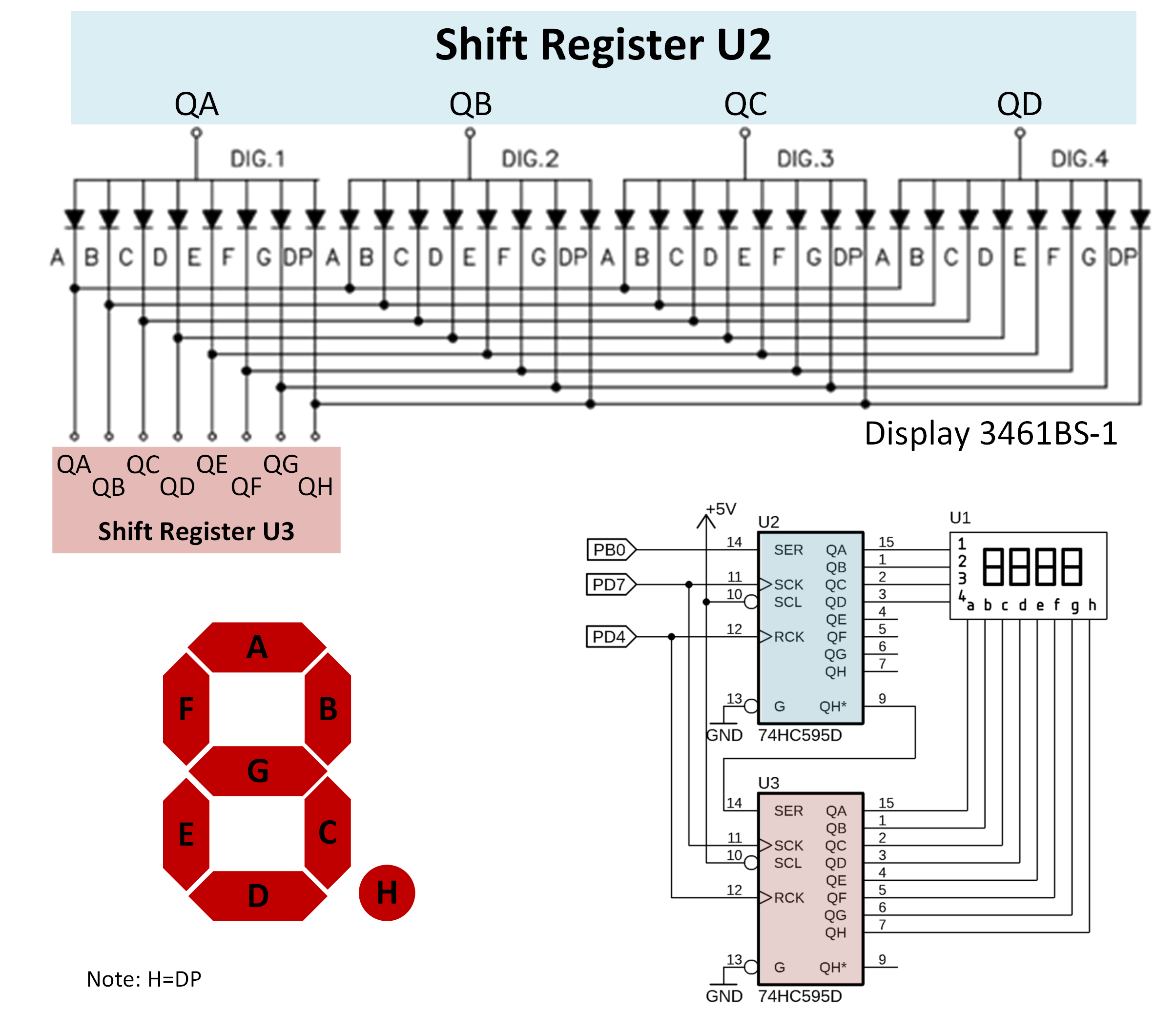
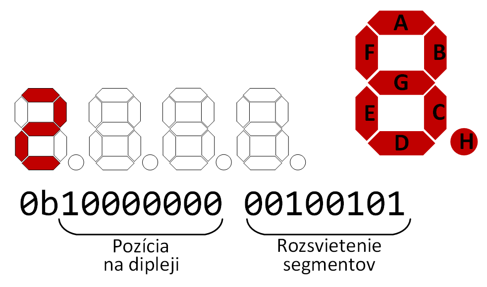
As shown in Fig. 3, register U2 selects the active digit position on the display, while register U3 controls the individual segments of the digit. For example, to display the number 2 at the first digit position, the binary sequence illustrated in Fig. 4 must be shifted sequentially into the registers, starting with the least significant bit (LSB first).
Procedure for Configuring the Shift Registers
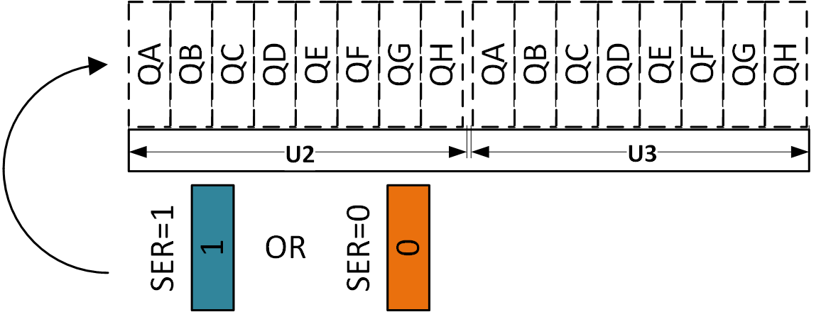
Register U2 uses outputs QA – QD to select the digit position on the 4-digit display. Register U3 uses outputs QA – QH to illuminate the corresponding segments of the 7-segment display. Together, both registers provide 16 outputs, with only 4 outputs of U2 connected to the display. The two cascaded registers can be visualized as a bookshelf that holds 16 books (Fig. 5). The right half represents register U3, and the left half represents register U2. A blue book represents a logic 1, and an orange book represents a logic 0. Books are always placed onto the shelf one by one from the left side.
To improve readability and clarity in the MCU code, define the following constants and helper macros:
#define SCK PORTD7
#define SER PORTB0
#define RCK PORTD4
#define SCK_H() PORTD|=(1<<SCK)
#define SCK_L() PORTD&=~(1<<SCK)
#define RCK_H() PORTD|=(1<<RCK)
#define RCK_L() PORTD&=~(1<<RCK)
Let us walk through the configuration process with a practical example: displaying the number 2 at the first digit position (Fig. 4). This requires shifting the 16-bit sequence 0b1000000000100101 into the registers bit by bit, as shown in Fig. 4.
Step 1
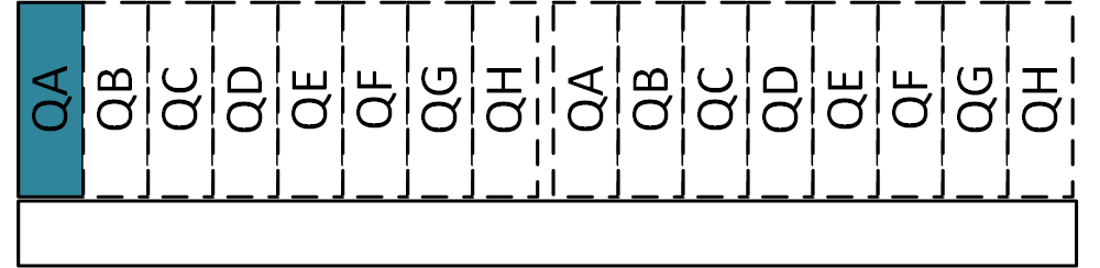
Data entry begins with the least significant bit (LSB). The LSB is 1, representing a blue book (logic 1). Prepare the bit by setting pin SER to logic 1. Push the book onto the shelf by generating a rising edge on clock pin SCK. Afterward, return SCK to logic 0 to prepare for the next bit.
The code for shifting the first bit into the register is as follows:
PORTB|=(1<<SER);
SCK_H();
_delay_us(1);
SCK_L();
_delay_us(1);
Step 2
In the second step, shift a logic 0 into the register—adding an orange book to the shelf. Prepare the bit by clearing pin SER to logic 0, then pulse SCK with a rising edge to shift the bit in.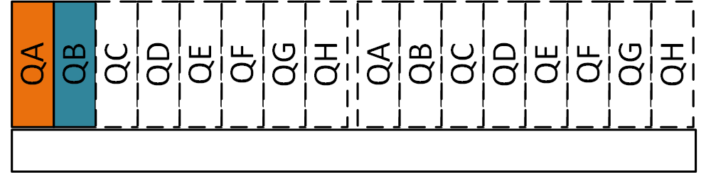
The code for shifting this value into the register is as follows:
PORTB&=~(1<<SER);
SCK_H();
_delay_us(1);
SCK_L();
_delay_us(1);
Steps 3 to 16
Repeat this process until all 16 books have been placed onto the shelf. Fig. 8 illustrates steps 3, 8, and 16 during the sequential loading of data into the shift register memory.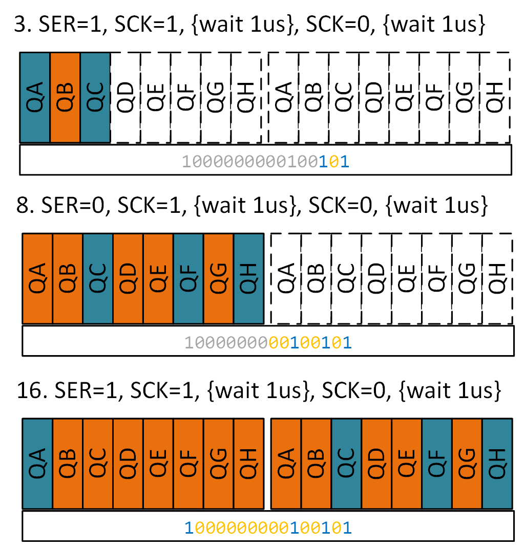
Latching Register Contents to the Outputs
The shelf represents the Shift Register shown in Fig. 1. Once filled with 16 bits (all 16 books placed), transfer the contents from the Shift Register to the Storage Register (latch). Trigger this transfer with a rising edge on pin RCK. As before, per the timing specifications, pull RCK back to logic 0 after a short delay. Because pin G ((OE) ̅) is pulled low (tied to GND), the contents of the Storage Register appear immediately on parallel outputs QA–QH of registers U2 and U3.
The corresponding code segment is shown below:
RCK_H();
_delay_us(1);
RCK_L();
_delay_us(1);
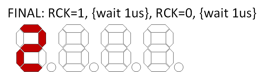
Executing this code illuminates the number 2 at the first position of the 4-digit 7-segment display (Fig. 9).
2. Equipment Used
- Hardware
- Mega Development Board 2 (MDB2)
- Multi-Function Shield
- PC
- Software
- Microchip Studio
3. Wiring Diagram
4. Tasks
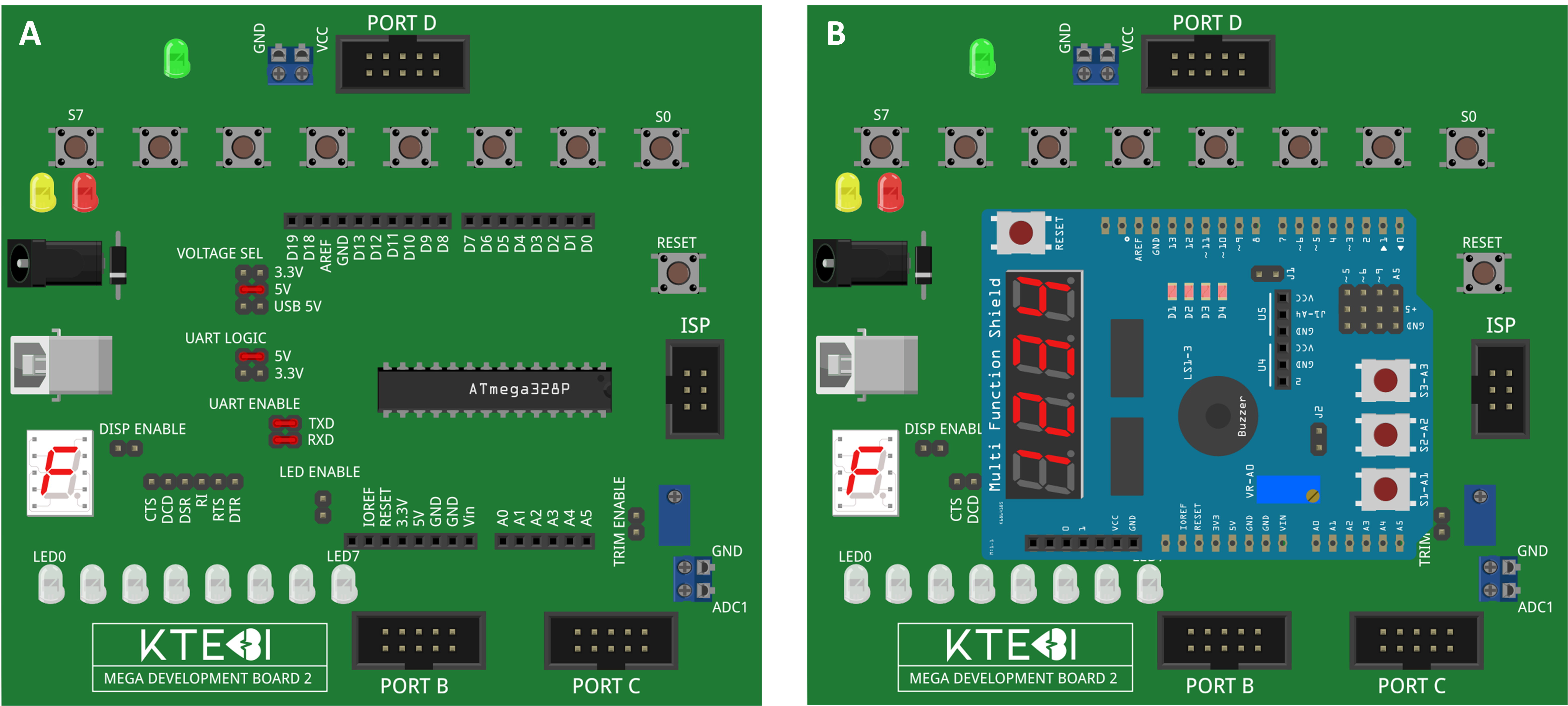
- Configure the jumpers on the MDB2 board according to the diagram in Fig. 10 A (jumper positions highlighted in red). Use an external power adapter. Mount the Multi-Function Shield onto the MDB2 development board as shown in Fig. 10 B.
- Write an MCU program in C to display the number 2 as shown in Fig. 9. Use the code snippets from the Theoretical Introduction as a reference.
- Write an MCU program in C to display the number 1234 across all four digits.
- Write an MCU program in C that initializes the display to 0. Pressing button S0 increments the display value, and pressing button S1 decrements it. The display range is 0 to 9999. Overflowing past 9999 wraps around to 0, and underflowing below 0 wraps around to 9999.
- Draw a program flowchart for Task 4.
- Evaluate the laboratory exercise, focusing on the MCU code implementation and any challenges encountered.